The semiconductor sector has undergone many changes in facility design, from conventional buildings to advanced modular cleanrooms. The changes have been necessitated by the demand for higher efficiency, flexibility, and cost savings in semiconductor facility design.
Traditional Semiconductor Facility Design
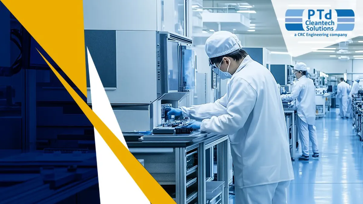
Historically, semiconductor manufacturing facilities were ‘stick-built,’ meaning they utilised traditional building principles. These original methods entailed building cleanrooms and controlled facilities on-site in a way specific to the requirements of the facility. This approach granted customisation opportunities but also faced issues of limited applicability. It became a challenge to stay on track with technological growth and process enhancement. Any sort of adjustments or expansions called for extensive downtime and resources.
Shift Towards Modular Cleanrooms
Against the constraints posed by the conventional designs, the sector has increasingly turned to modular cleanrooms. These are factory-built modules constructed off-site and installed on-site, providing a scalable and flexible replacement for conventional construction. Modular construction offers a number of benefits:
- Speed of Construction: Modular cleanrooms are faster to deploy compared to conventional construction since parts are pre-designed and take less time to assemble on site.
- Cost Effectiveness: Standardisation and off-site assembly of modules minimise material wastage and labour.
- Flexibility and Scalability: Modular designs are easily reconfigurable and expandable, making it possible for facilities to quickly respond to changing technological needs and production demands.
This shift to modular cleanrooms represents a dramatic change in the semiconductor facility design.
PTD Cleantech Solutions: The Torchbearers of Modern Facility Design
PTD Cleantech Solutions (PTD-CS) is a global design and engineering firm that is at the helm of semiconductor facility design evolution. Dedicated to controlled environments for high technology and life science markets, PTD-CS provides full-service offerings in the form of engineering, project management, construction management, and commissioning qualification validation assistance.
Their technical knowledge of cleanroom technology and controlled environments provides customers with personalised solutions that meet strict industry requirements. Combining modular cleanroom design, PTD-CS responds to the needs of the industry for flexible, effective, and economical facilities. This strategy speeds up project schedules and streamlines operational efficiency which enables semiconductor manufacturers to sustain their competitive advantage in an ever-changing marketplace.
PTD-CS’s focus on innovation and sustainability is also embodied in design approaches that include energy-efficient systems and eco-friendly materials. Such commitment is also in line with the trend towards greener approaches in the industry, making sure that semiconductor facility design is attuned to existing technological requirements while also positively affecting environmental objectives.
The transition from conventional to modular cleanrooms represents a major development in semiconductor facility design. PTD Cleantech Solutions is at the forefront of this development with effective solutions that meet the requirements of the semiconductor market. Adopting advanced design concepts will be instrumental in maintaining growth and competitiveness within the industry.