Due to its advanced on-site manufacturing infrastructure and design capabilities, India is becoming a significant node in the global semiconductor ecosystem. Semiconductor facility design is one of the deciding arenas where regulatory integration and cleanroom engineering are redefining India’s strategic platform as the heart of this evolution.
Localised Cleanroom Implementation and Strategic Growth
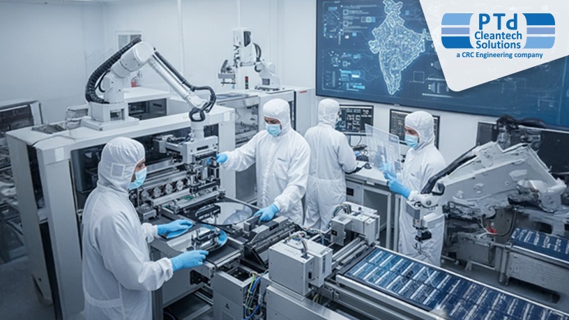
One example is the historic Micron facility in Sanand, Gujarat. 500,000 square feet of carefully verified cleanroom space make up its first phase, which was created using contemporary EPC methodology that incorporates 4D BIM and modular construction techniques (cleanroom technology). This demonstrates how Indian semiconductor facility design is incorporating international best practices into regional frameworks to facilitate deeper localisation and quicker project execution.
This technical change is further enhanced by India’s policy ecosystem. To strengthen domestic semiconductor capabilities, the India Semiconductor Mission is implementing generous incentives, such as up to 50% funding for advanced CMOS fabs, and support for local fabrication clusters (cleanroom technology). By integrating India into the semiconductor manufacturing value chain with robust infrastructure and cleanroom-dependent production, these programs are pushing the nation past labour arbitrage.
Bridging Design Talent and Cleanroom Manufacturing
India’s design talent is a high-value addition. According to The Times of India, the nation is home to about 20% of the world’s semiconductor design engineers. Cleanroom manufacturing now needs to come together with this depth of knowledge. Indian EPC and cleanroom experts like Pophen Technology India and Semicon Fab Technologies are helping to integrate cutting-edge cleanroom systems and components into regional projects (cleanroom technology). One important strategic enabler is the synergy between cleaner-room execution and design depth.
It is anticipated that controlled-environment cleanroom capabilities will be integrated from the beginning as the Tata Semiconductor Assembly and Test (TSAT) facility in Assam develops, which is expected to become India’s first domestic semiconductor assembly and test site (Wikipedia). Every such development demonstrates how India’s semiconductor facility design is evolving holistically, fusing domestic supply chains with controlled environments.
Future-Ready Infrastructure and Cleanroom Collaboration
In the future, India has suggested establishing a “Taiwan-inspired” shared R&D and cleanroom pilot line in the Dholera area of Gujarat. By sharing cleanroom infrastructure for training and prototyping, this centre hopes to assist established players and start-ups alike (Digitimes Asia). The future of semiconductor facility design with shared infrastructure will be shaped by such initiatives, which will ease early-stage access to cleanroom environments and boost collaborative innovation.
India’s determination to upgrade its historic research facilities, such as the Semi-Conductor Laboratory (SCL) in Mohali, with a $2 billion investment indicates a national goal to establish fundamental cleanroom infrastructure for crucial research and chip fabrication (Wikipedia).
Cleanrooms as Strategic Anchors
All things considered, India’s contribution to the global semiconductor industry is growing from design services to integrated production, with cleanroom architecture at its heart. The semiconductor facility design, from Micron’s cleanroom phase in Gujarat to shared R&D pods in Dholera and updated national labs in Mohali, is increasingly influencing independence and competitive differentiation.
India is currently developing an ecosystem in which its engineering talent and manufacturing goals are perfectly matched with high-precision cleanroom environments. Not only will chips shape the country’s future in the global semiconductor supply chain, but the cleanrooms that enable them will also play a significant role.