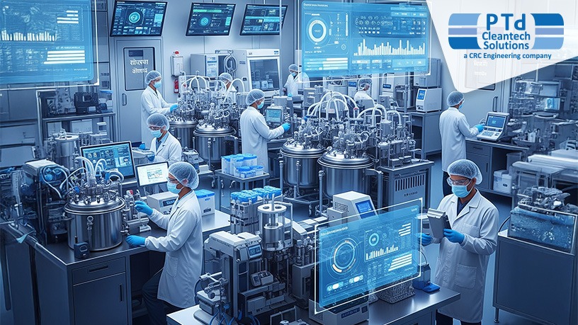
How Environmental Monitoring Systems Evolve in High Risk Cleanrooms

As industries strive for increased accuracy and dependability, environmental monitoring systems have become very important to the development of high-risk cleanrooms. Controlled environments are more important than ever in industries like microelectronics and pharmaceuticals.
The Hidden Science of Pressure Cascades: Designing Flow Barriers That Actually Work

One of the most effective yet frequently misinterpreted tools in controlled environment engineering is the pressure cascade. The way air flows through a space determines whether it is a bioprocessing suite, a pharmaceutical cleanroom, or a facility for next-generation cell therapy. It is essential to prevent contamination. It is no coincidence that the air is forced from one area to another by a subtle gradient.
Understanding Contamination Beyond Particulates: Managing Risks in Cleanrooms

Particle control has long been linked to cleanrooms. Engineers and quality experts have been working to reduce dust, fibres, microscopic debris etc., for decades. Even though these problems are still very important to address, there are now many more contamination risks that modern cleanrooms must deal with than just particulates.
Electrostatic Discharge (ESD) Mitigation: Best Practices Beyond Flooring

Electrostatic discharge (ESD) is one of the most persistent and often underestimated threats in controlled environments such as semiconductor, electronics, precision manufacturing facilities, etc. ESD flooring is merely one layer of a much larger defence strategy, even though it is still a crucial component of protection.
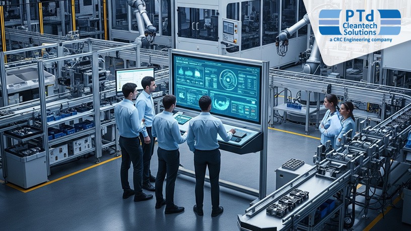
Smart Cleanrooms: The Role of IoT in Real-Time Control

Smarter and more efficient production environments are more important than ever in the industrial landscape of today. Cleanrooms are more than just sterile areas kept up to date with manual supervision and static controls. They are now intelligent and responsive ecosystems that continuously monitor and optimise their own performance due to Internet of Things (IoT).
Integrating AI and Machine Learning into Cleanroom Environmental Monitoring

In highly regulated industries such as pharmaceuticals, semiconductors, and biotechnology, maintaining the integrity of the atmp design of a cleanroom environment is non-negotiable. Controlled parameters, such as particulate counts, air pressure differentials, temperature, humidity, and microbial load, must remain within tight bounds.
The Role of Data Analytics in Facility Validation and Monitoring
Data analytics has become a game-changing tool for making sure that facilities adhere to the strictest safety and operational efficiency standards. Facility validation and continuous monitoring are essential procedures that preserve product quality and human health in sectors like pharmaceuticals, biotechnology, semiconductors, etc. They are also merely legal requirements.
The Rise of Vendor-Integrated Turnkey Solutions in Precision Manufacturing
Vendor-integrated turnkey services have become more popular in the dynamic precision manufacturing industry due to the need for effective and affordable solutions. These all-inclusive services give manufacturers a smooth transition from idea to production by covering design, engineering, procurement, and installation.
India’s Cleanroom Strength within Global Semiconductor Supply Chain
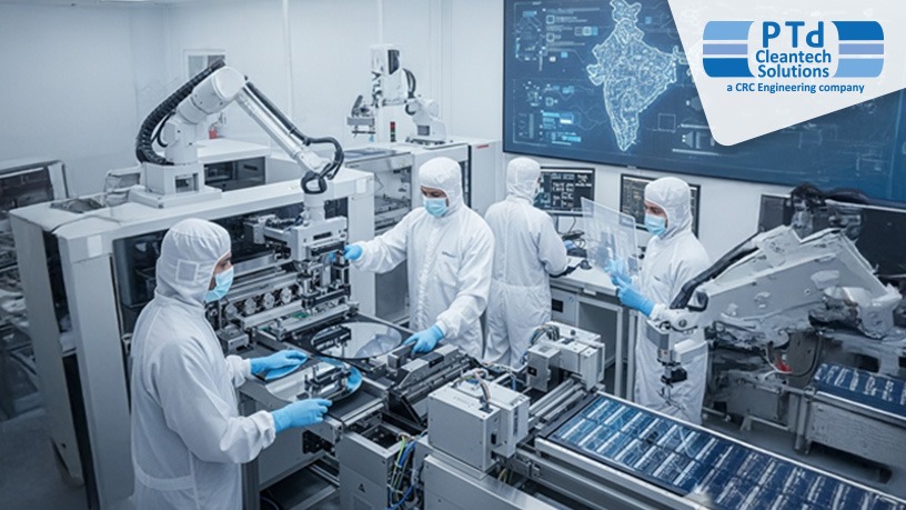
Due to its advanced on-site manufacturing infrastructure and design capabilities, India is becoming a significant node in the global semiconductor ecosystem. Semiconductor facility design is one of the deciding arenas where regulatory integration and cleanroom engineering are redefining India’s strategic platform as the heart of this evolution.
Microelectronics Manufacturing: How Cleanroom Design Impacts Yield
The smallest particle can make a huge difference between a working device and an expensive flaw in the high-stakes world of microelectronics manufacturing. Cleanroom design is more important than ever because manufacturing tolerances have reached the nanometre scale as devices have started to get smaller and more complex.