Evident from its name, OSAT ( Outsourced Semiconductor Assembly and Test ) refers to a specialised group of individuals or a company that renders services revolving around semiconductor design and supply. OSAT Design further streamlines the process by providing an overall design to facilitate the entire process of creating a semiconductor facility or converting an existing facility into one.
OSAT (Outsourced Semiconductor Assembly and Test) Design asserts its relevance as it facilitates concentrating on design and innovation, leaving the last stages of the execution to the specialised service providers.
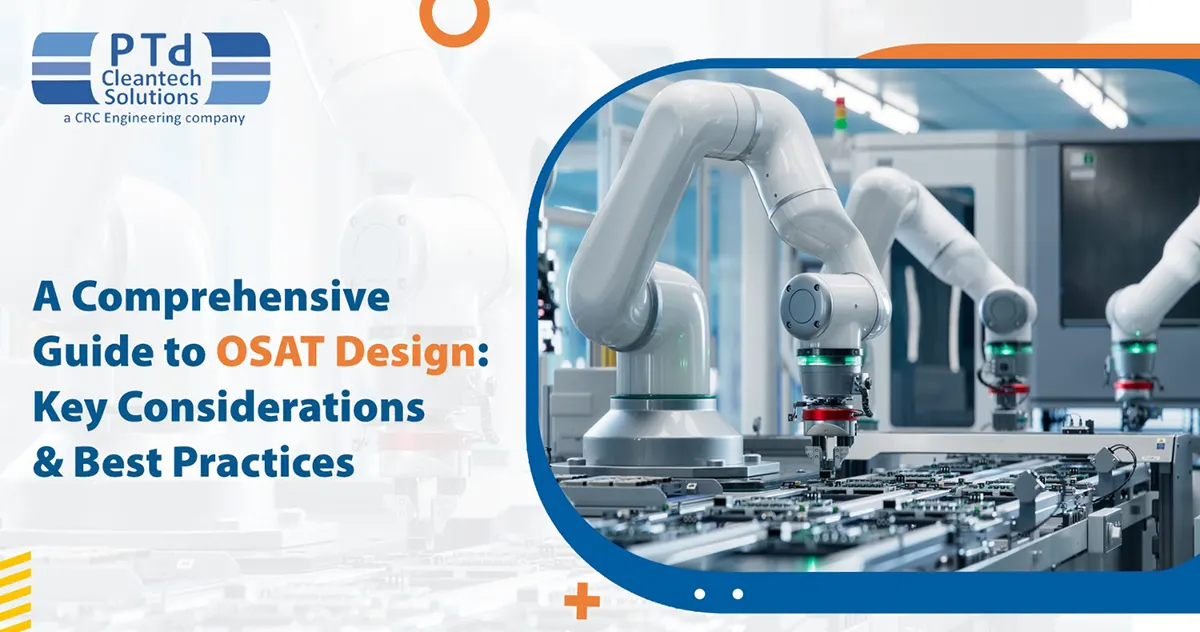
While rendering services in the arena of semiconductor engineering there are certain best practices that should be followed to maximise the output of the production line.
With the rise of automation, the integration of artificial intelligence is pretty much prevalent in a lot of industries. The same is the scenario for semiconductor facility design, where A.I. integration has taken the entire supply chain to new heights of productivity. Integrating artificial intelligence into the process also ensures the maintenance of top-notch standards both in terms of quality and adherence to deadlines.
Thorough testing for quality analysis should be implemented to ensure seamless applications of the semiconductor facility design. This includes ensuring the proper functioning of everything starting from contingency management to safety measures. Testing every aspect of the plan is inherently necessary for the seamless functioning of the supply chain. Semiconductor facility consultants can use digital twins to simulate and develop complex testing procedures. Integration of AI into these procedures can improve testing procedures and predictive analytics, thereby reducing expenses and time drastically.
Ensuring the sustainability of a semiconductor facility is one of the top priorities for OSAT Design. Sustainability plays not only one but multiple pivotal roles in a seamless production process. Sustainability ensures restoration and reuse of conventional resources and hence ends up being cost-effective.
Apart from the cost-effectiveness, ensuring sustainability also adds up to the value of Corporate Social Responsibility. CSR initiatives portray that the company is concerned with the environment and is making an effort to impact it positively. This also paves the way for multiple government grants and aids.
One of the most important things that a semiconductor facility design should ensure is leaving room for customisation. With the increasing demands of the market, a semiconductor facility keeps the capacity to quickly catch up with the requirements as it reduces operation time and maintains the quality of execution. However once when the demand exceeds the supply, the facility should have ample space for an upgrade and further customisation, without having to scrap down and redo the entire process.
As a semiconductor facility consultant, one of the most important things that should be ensured for OSAT design is the end-to-end capability of design and testing facilities. The end-to-end experience in design and testing should greatly lower the likelihood of production process delays and interruptions. High-end research and development should also be a part of the paraphernalia of a semiconductor facility consultant.
The market for OSAT is walking towards an incredible rise as the demand is increasing for leading-edge semiconductor technology.
This would allow the service providers to seize the market opportunity based on the booming industry and by matching the strengths with the needs of the semiconductor clients through R&D, personnel management, or enhanced packaging.
To succeed in this fast-changing environment, the semiconductor facility consultants who seek to capitalise on this opportunity will have to segment the market, identify key opportunities, and develop targeted plans based on actionable market intelligence, of which our experienced team can provide thorough insights.
Office No. 11&12,
L-Square Building,
Sanghvi Nagar,
Near Parihar Chowk,
Aundh, Pune 411007
Symphony IT Park, Office No. 206, Tower B1, Level 2,
Nanded City, Sinhgad Road, Pune MH – 411068
2024 © ptd-cs.com - All rights reserved
The brochure will be automatically delivered to your email inbox.